
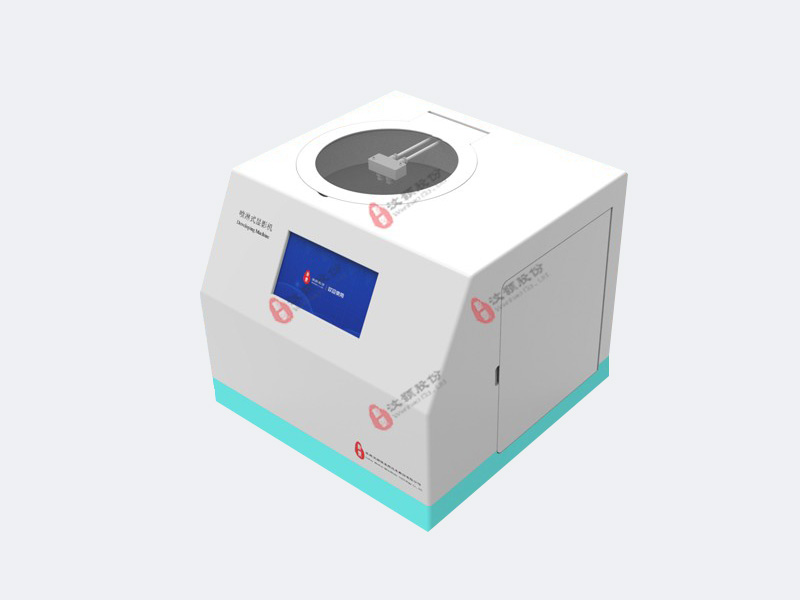
Developing Machine
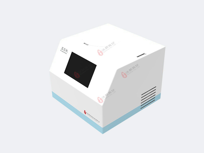
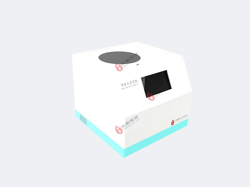
The developing machine is a programmed instrument for developing photolithographic silicon wafers, which can meet the improvement of various details of silicon wafers. The developing machine chamber is an erosion safe cavity, which can naturally infuse a comparable measure of creating arrangement as indicated by the details of the silicon wafer, and has the capacity of mirroring counterfeit shaking, and can consequently eliminate the waste fluid.
The designer is intended for developing machine manufacturer and developing machine supplier and is utilized in the advancement interaction in lithography processes
The machine can supplant the manual improvement in the assembling system of the microfluidic chip, beats the wild advancement season of the manual turn of events, and diminishes the harm of the silicon wafer/chip by the developing machine manufacturer and developing machine supplier
There are the principle elements of the developing machine :
1) The shaking recurrence of the developing machine can be set to guarantee adequate contact between the creating arrangement and the silicon wafer, and to work on the creating impact and quality.
2) The creating plate lifting position can be precisely set by the created developing machine manufacturer and developing machine supplier in this way deciding the entering measure of the creating arrangement, and staying away from misuse of the creating arrangement.
3) The developing machine manufacturer and developing machine supplier can be consequently added and released, and can be deftly supplanted.
4) Friendly human developing machine interface plan to guarantee the administrator’s insight and wellbeing.
5) Good conveyability and simple to move in the lab,
FAQ
What are the processes involved in developing machine photolithography?
Photolithography is the most common way of moving mathematical shapes on a cover to the outer layer of a silicon wafer. The means the photoresist developing machine associated with the photolithographic cycle are wafer cleaning; boundary layer arrangement; photoresist application; delicate baking; cover arrangement; openness and advancement; and hard-baking.
The developing machine manufacturer and developing machine supplier utilizes three essential interaction steps to move an example from a cover to a wafer: coat, create, uncover. The example is moved into the wafer’s surface layer during a resulting cycle.
Wafer Cleaning, Barrier Formation and Photoresist Application
In the initial step, the developing machine wafers are synthetically cleaned to eliminate particulate matter on a superficial level as well as any hints of natural, ionic, and metallic pollution. In the wake of cleaning, silicon dioxide, which fills in as a boundary layer, is saved on the outer layer of the developing machine wafer.
After the development of the SiO2 layer, the photoresist developing machine is applied to the outer layer of the wafer. Rapid outward spinning of silicon wafers is the standard technique for developing machine coatings in IC assembling. This strategy, known as “Twist Coating,” creates a flimsy uniform layer of photoresist on the wafer surface.
What is the development of photolithography for a photoresist developing machine?
Advancement
The uncovered wafers are created in dunking showers or in splash processes. While the plunging showers of photoresist developing machine permit the improvement of various wafers all at once, in splash advancement one wafer is handled after another. As in oppose the covering processes the wafer is put on a throw and showered with creating synthetic compounds while photoresist developing machine pivoting at low rpm. Ensuing the wafer improvement process is halted with water.
Some advantages of the developing machine development in contrast to dipping baths are:
1) smallest structures can be developed
2) the chemical is renewed steadily
3) the amount of chemicals is much less
4) depending on the type of resist – negative/positive – uncovered regions are soluble or insoluble in creating synthetic substances and a designed wafer stays after advancement. The openness causes a synthetic response in the opposite in this way that the sensitizer frames a corrosive which is killed by the developing machine manufacturer and developing machine supplier.
Since potassium hydroxide or sodium hydroxide leave residuals on the photoresist developing machine wafer, synthetic substances without metal particles, such as TMAH (tetramethylammonium hydroxide), are utilized. An extra tempering solidifies the developing machine to ensuing engraving cycles or particle implantation.
The developing machine must be reviewed subsequently. In precise frequency of light the consistency of the layer can be reviewed as well as terrible centering or agglomeration of stand up to. In the event that designs are too dainty or too wide the opposition must be eliminated and the cycle must be rehashed. The developing machine design must be changed exactly to the layer underneath or the cycle must be rehashed too.
What is inspection in photolithography for a photoresist developing machine?
Investigation
The photoresist developing machine must be reviewed a short time later. In precise rate of light the consistency of the layer can be reviewed as well as terrible centering or agglomeration of stand up to. On the off chance that photoresist developing machine designs are too slim or too wide.
The photoresist developer machine must be eliminated and the cycle must be rehashed. The photoresist developer machine design must be changed definitively to the layer underneath or the interaction must be rehashed too. Different arrangement marks are utilized to research the change and the line width.
Light beams occur in opposite directions onto the wafer and won’t be reflected into the target from edges. Along these lines the edges, developing machine manufacturer and developing machine supplier made the machine to show up as dim lines which can be utilized to compute the line width and distance to adjoining lines.
What is resist in photolithography for a photoresist developing machine ?
A photoresist (likewise referred to just as an oppose) is a light-touch material utilized in a few cycles, like photolithography and etching, to shape a designed covering on a surface. This interaction is significant in the developing machine manufacturer and developing machine supplier industry.
The interaction starts by covering a substrate with a light-touchy natural material. A photoresist developer machine is then applied to the surface to obstruct light, so that main exposed areas of the material will be presented to light. A dissolvable photoresist developer machine, is then applied to the surface.
On account of a positive photoresist, the photograph touchy material is corrupted by light and the photoresist developer machine will break down away the locales that were presented to light, leaving behind a covering where the veil was set. On account of a negative photoresist, the photosensitive material is reinforced by light, and the photoresist developer machine will break up away just the districts that were not presented to light, leaving behind a covering in regions where the veil was not set.
After It has been moved into the layer underneath in carve processes, or after the photoresist developer machine cover was utilized in particle implantation, the photoresist developer machine must be taken out. This is finished with grating synthetic compounds (remover), in a dry engraving step or with solvents. As dissolvable CH3)2CO can be utilized since it doesn’t consume different layers on the wafer. Because of a dry engraving cycle or particle implantation the oppose could be solidified, with the goal that solvents can’t eliminate it.
For this situation the photoresist developer machine can be taken out with a remover dilustion at around 80 °C in a plunging shower. In the event that the photoresist developer machine has been heatened over 200 °C even the remover can’t eliminate it. For this situation the It must be taken out in an ashing interaction.
Under oxygen surrounding a gas release is touched off by high recurrence, along these lines vigorous oxygen molecules are created. These iotas can debris the photoresist developing machine buildup free. Nonetheless, charged particles can be sped up in the electric field a developing machine
harm to the wafer surface.