
Specification for chip fabrication drawings
Dear customers,
Hello! In order to confirm the chip processing drawings more conveniently and efficiently, please try your best to design drawings according to the following specifications, thank you!
Drawing format requirements:
3D general format. Step /.IGS /.x_t
2D general format. DWG /.dxf
If you use SolidWorks drawings, save as “Parasolid Binary(*.x-b)”
GDSII, CIF, TDB drawn with L-Edit
PDMS, pure silicon chip:
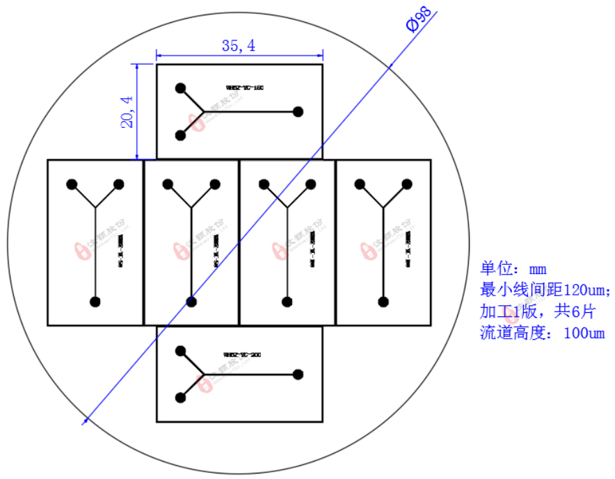
1. Drawing scope: circle with diameter of 98mm;
2. If the runner has more than one height, please draw in layers, fill the height with different colors, and note;
3. The border of a single structure must be drawn, and it is recommended that the border of the structure be at least 5mm away from the border;
4. If it is necessary to cast PDMS chip, please note the overall PDMS thickness, which is recommended to be 3-4mm;
5. Note the hole diameter of PDMS inlet and outlet sample mouth, which is recommended to be 0.5mm in diameter, 0.5*0.7mm in matching stainless steel connector, and 0.5*0.9mm in PTFE catheter;
6. Remarks: drawing unit, minimum line spacing, processing quantity.
PDMS, pure silicon chip drawings design
Glass chip:
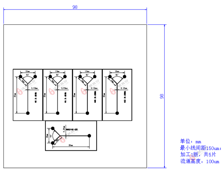
1. Drawing scope: 98*98mm square;
2. If the runner has more than one height, please draw in layers, fill the height with different colors, and note;
3. The border of a single structure must be drawn, and it is recommended that the border of the structure be at least 5mm away from the border;
4. Remark: The hole diameter of the inlet and outlet is 1mm, and it is recommended to glue the 1/16peek connector and base. If the base is glued, the distance between the center of the two injection ports should be greater than 7.5mm.
5. Remarks: drawing unit, minimum line spacing, processing quantity.
Specification for glass drawing design
PMMA chips:
PMMA chips are processed by CNC machine tools, and standard CAD drawings or drawings in STEP /.IGS /.x_t format are provided.
Dear customers,
Hello! In order to confirm the chip processing drawings more conveniently and efficiently, please try to design the drawings according to the following specifications: only provide the CAD plan, indicating the dimension parameters of the channel, and marking the corresponding depth of the channel. The area of the drawing is a circle with a diameter of 4 inches (about 10cm). If the drawing is complicated, please mark several sizes. Note the unit, thank you!
Schematic diagram of chip channel structure
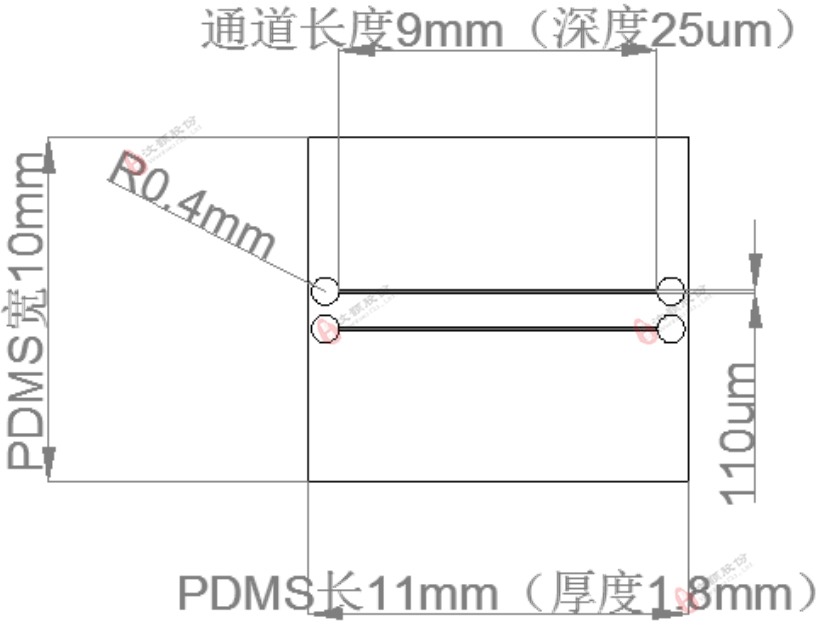
FIG. 1 Structure diagram of chip channel, the overall size of the chip is 10*11mm
Schematic diagram of chip base electrode structure
FIG. 2 Schematic diagram of chip base electrode structure, the overall size of the base is 13*19mm


tadalafil 5mg https://canadianpharmaceuticalsonline.home.blog/
You mentioned that really well.