Lithography technology graphics transfer process
Photoetching or Lithography is an image copying technique that accurately copies a lithographic mask onto a photoresist coated on a silicon wafer using the principle of changing the characteristics of the photoresist. Then, using photoresist as a mask protection, selective processing (etching or implanting) on the mask layer on the surface of the wafer, thereby obtaining a corresponding pattern structure on the wafer, the main process is: first ultraviolet light The photoresist is irradiated onto the surface of the silicon wafer coated with a photoresist film to cause a chemical reaction of the photoresist in the exposed region, and then the photoresist is dissolved and removed in the exposed region or the unexposed region by the developing method (the former is called A positive photoresist, the latter is called a negative photoresist, so that the pattern on the mask is copied onto the photoresist film, and finally the pattern is transferred to the substrate by etching or the PDMS is formed by the engraving technique. chip.
Lithography
Wenyi provides lithography such as electron beam lithography, step lithography, contact lithography, etc., with a line width of up to 10 nanometers, and a variety of lithography technology combined with advanced lithography concepts to achieve customer lithography of different sizes. demand.
Spin coating technology
The quality of spin coating directly affects the effect of lithography. Wenhao provides professional spin coating technology, the sample covers 1cm2 to 12 inch wafers, spin coating uniformity, high adhesion, good finished product quality.
Etching process
The etching process mainly includes wet etching and dry etching. Wet etching is a kind of pure etching, which uses liquid chemical reagent to react with the material to be etched to form a soluble compound, which achieves the purpose of etching. It has excellent selectivity, and the current film will stop after etching, without damaging the following. A film of another layer of material is isotropic, and the width of the lateral etch is close to the depth of the vertical etch. Therefore, there is a certain deviation between the pattern of the upper photoresist and the pattern etched on the underlying material.
Dry etching is the use of plasma to interact with the material to be etched (physical bombardment and chemical reaction) to remove the material not protected by the photoresist for etching purposes. The dry etching is divided into three types: physical Etching (sputter etching), chemical etching, physicochemical etching. Dry etching can perform anisotropic etching, but selective etching is not possible.
At present, in the pattern transfer, silicon nitride, polysilicon, metal and alloy materials are mostly dry etching techniques, while silicon dioxide is mostly wet etching, and sometimes metal aluminum is also wet etching.
Featured business
Wenhao has a complete microfluidic chip processing equipment and an experienced team of chip engineers to provide standard chip and custom chip processing services. Customers can design microfluidic chips or commission microfluidic chips according to their own needs. Design and processing.
Wenhao currently offers photoresist molds (in general aspect ratio of 1:1 to 3:1), pure silicon molds (in general aspect ratio of 10:1 to 15:1), glass chips, gold-plated/electrode chips, Customized design and processing of PDMS chips, mass production of PDMS chips, and related services such as chip masking, etching, cutting, punching, sealing, encapsulation, and hydrophobic treatment.
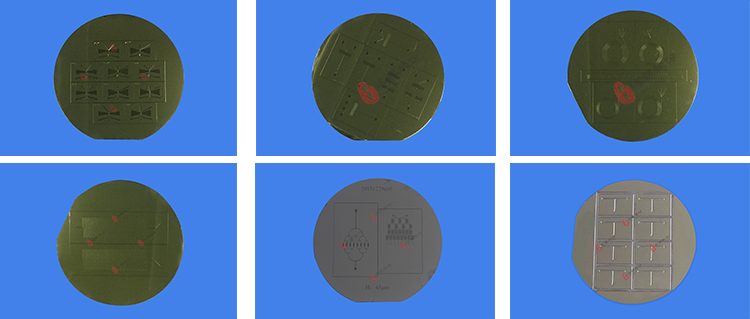
First, the silicon mold
Processing capacity: 2 inch silicon wafer, 3 inch silicon wafer, 4 inch silicon wafer (common), 5 inch silicon wafer lithography processing, minimum line width 5μm, height 5μm to 400μm controllable, error 5%-10 %;
Types of photoresist: imported SU8 series, domestic SU8 series, imported AZ50XT, AZ9260;
Advantages of photoresist mold: easy patterning and convenient use, currently the main processing technology for microfluidic mold processing:
Single layer structure: a photoresist mold height
Double layer structure: one photoresist mold two heights
Three-layer structure: one photoresist mold three heights
Second, the glass chip
Advantages of glass chip: high processing efficiency, high precision, easy to use, no pollution, high chemical inertness; high light transmission, can directly observe chemical or cellular reactions; high temperature resistance and high resistance, can be separated by high pressure electrophoresis; The mechanical stability allows the transport of liquids in the microchannels with high hydrostatic pressure.
Typical applications of glass microfluidic chips: gene sequencing chips, optical analysis chips, microfluidic chips, sperm counting cells, cell counting plates, chemical synthesis, etc.
Below are some tech:
1. Glass wet etching
Processing capacity: controllable from 5 to 250μm depth; channel width = mask design width + 2 * channel depth;
When processing, it must be processed in a full-page, the substrate size is 10cm*10cm square, and it is cut after processing.
Advantages: the surface roughness is small, and the inner wall of the channel is smooth when the channel is shallow;
Disadvantages: The depth is difficult to control accurately. When the channel depth is greater than 50μm, the inner wall smoothness is deteriorated, and the aspect ratio must be greater than 2:1.
2, Glass CNC machining
Processing capacity: controllable with depth above 100μm, controllable line width of 20μm or more, processing error within 5%, and outer edge cutting error within 20μm;
Advantages: the depth and width of the pipeline are relatively large, and the processed channel has a high flatness;
Disadvantages: high cost, the pipe section is usually V-shaped or trapezoidal.
3, Glass laser processing
Processing capacity: controllable above 100μm depth, controllable line width 20μm or more, machining error within 10%, and outer edge cutting error within 40μm.
Advantages: low cost, large depth and width of the pipeline;
Disadvantages: The roughness is large, and the cross section of the pipe is usually V-shaped or trapezoidal.
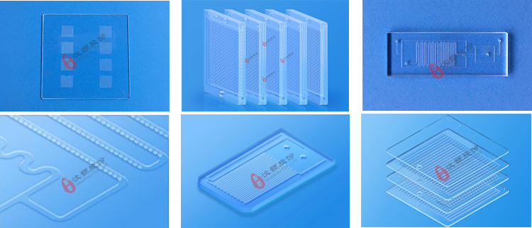
Third, PDMS chip
Processing capacity: can be engraved, cast, cut, punched, processed ordinary PDMS chip or custom cavity according to customer requirements.
PDMS chip processing is usually done by soft lithography. Templates are usually used. The most common and frequently used templates are SU-8 molds, and plastic molds such as metal molds and PMMA can also be used.
PDMS chip single engraving can meet the aspect ratio of 1:1~10:1, the engraved thickness is 10 microns to 2 cm, the perforation diameter is 0.4 mm to 10 mm, and finally sealed with glass, PDMS and other materials. .
Standard deviation of manufacturing:
1) Channel height: △h=±5% channel height
2) Accuracy of height features: ±5% channel height
3) Channel sidewall verticality: ±3°
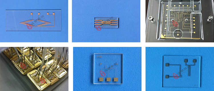
Fourth, gold-plated / electrode chip
Processing capacity: It can process gold-plated, platinized, ITO and other electrode chips with a lower limit of 50μm and a spacing of 50μm.