The new chemically amplified negative image SU-8 adhesive is a negative, epoxy resin, near-ultraviolet photoresist, which overcomes the low aspect ratio caused by UV lithography in the ordinary photoresist. It is very suitable for the Preparation of high aspect ratio microstructures. SU-8 photoresist has deficient light absorption in the range of near-ultraviolet light (365nm-400nm). The exposure of the entire photoresist layer is uniform, so a thick film with vertical sidewalls and a high aspect ratio can be obtained Graphics. It also has good mechanical properties, chemical resistance, and thermal stability. SU-8 is cross-linked after being exposed to ultraviolet radiation. It is a chemically enlarged negative adhesive that can form complex patterns such as steps, and SU-8 adhesive is non-conductive and can be used directly as an insulator during electroplating. Due to its many advantages, SU-8 glue is gradually being used in MEMS, chip packaging, and micro-processing. It has become a new technology in micro-machining that uses SU8 photoresist to fabricate microstructures and micro-parts with a high aspect ratio.
SU 8 photoresist cleaning process before photolithography
The substrate needs to be cleaned before spin-coating the photoresist to achieve a better photolithography effect, The typical cleaning method is to soak in a mixed solution of concentrated sulfuric acid and hydrogen peroxide, then rinse with deionized water and blow dry with nitrogen. In addition, it can also be cleaned by reactive ion etching or plasma surface cleaner.
SU 8 photoresist lithography process
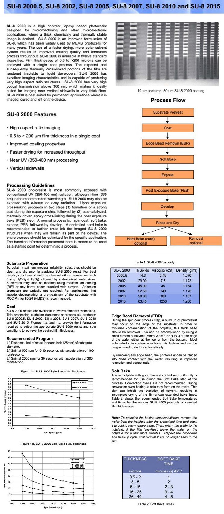
The SU-8 photoresist component is spin-coated on the substrate with a thickness of several to several hundred microns. The coated wafer is pre-baked and cooled to room temperature. During the drying process, a heating plate with uniform heating and precise temperature control is preferred; Do not use a blast drying oven to prevent the preferential curing of the photoresist surface from preventing the volatilization of the inner photoresist solvent. After cooling, the negative photomask is brought into contact with the coated wafer and exposed under the conditions of a mercury lamp’s ultraviolet radiation dose of 10-250mJ/cm². After the exposure is over, select the appropriate baking temperature and time. The wafer is immersed in a developing solution for development and then dried with nitrogen.
Advantages of SU-8 photoresist
1. SU-8 photoresist has deficient light absorption in the range of near-ultraviolet light (365nm-400nm), and the exposure amount obtained by the entire photoresist layer is uniform, and a vertical sidewall and high aspect ratio and thick film graphics;
2. SU-8 photoresist has good mechanical properties, chemical resistance, and thermal stability;
3. SU-8 is cross-linked after being exposed to ultraviolet radiation. It is a chemically enlarged negative adhesive that can form complex patterns such as steps;
4. SU-8 glue is not conductive and can be used directly as an insulator during electroplating.
Due to its many advantages, SU-8 glue is gradually being used in MEMS, chip packaging, and micro-processing. It has become a new technology in micro-machining that uses SU8 photoresist to fabricate microstructures and micro-parts with a high aspect ratio. In the processing of microfluidic chips, SU-8 is mainly used to process PDMS microfluidic chips by rapid molding.