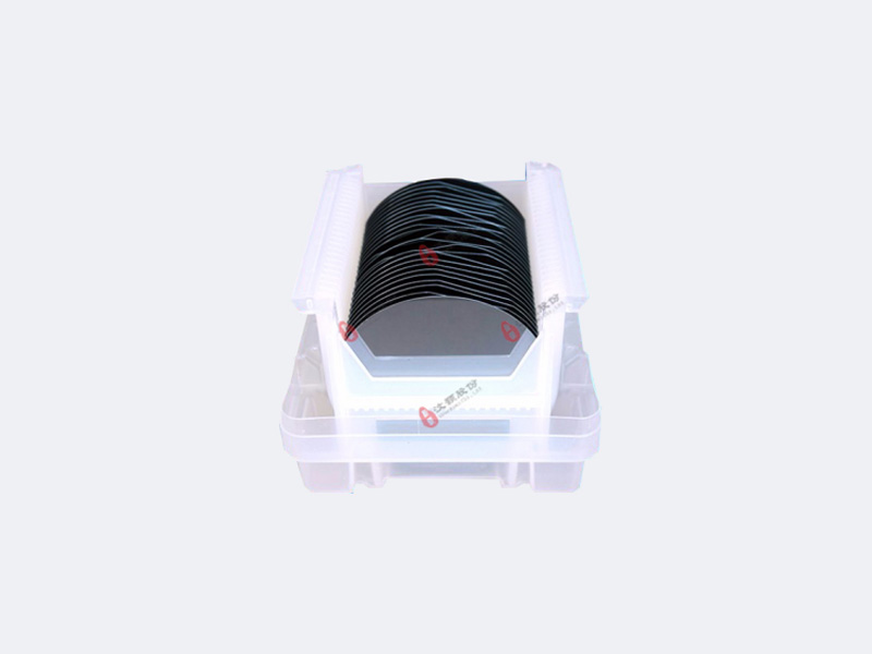
Brief introduction of polished silicon wafers
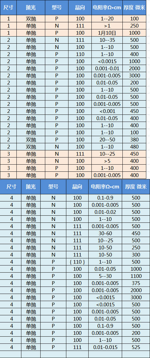
Size 1 inch to 4-inch range, thickness 0.2 mm, 0.4 mm, 1 mm, 1.2 mm and other thickness, single-sided polishing.
Parameters and applications of polished silicon wafers:
| Parameter Type
|
Sitechnical specification
|
| Product size | 1-4inches |
| Method of growth
|
Czochralski single crystal (CZ)
|
| Surface finish
|
one-sided finish
|
| Diameter tolerance
|
100.2±0.3mm |
| Doping type
|
dopant (phosphorus or boron)
|
| Crystal Orientation
|
100 111 |
| Resistivity
Ω |
<0.0015 Ω.cm 0.001-0.5Ω.cm 1-10Ω.cm |
| Flatness
TIR |
<3um |
| Warp
TTV |
<10um |
| Curvature
BOW |
<10um |
| Polishing roughness
Ra |
<0.5nm |
| Granularity
Pewaferr |
<(for size>0.3um) |
| Thickness
um |
please consult
|
| Application | iIt is used to fabricate microfluidic chips, such as photolithography process, synchrotron radiation sample carrier, LPCVD/PECVD film as the substrate, magnetron sputtering sample, XRD, SEM, AFM, infrared spectrum, as well as in the Molecular beam epitaxy of Crystal Semiconductor.
|