
First, we need to make a mask.
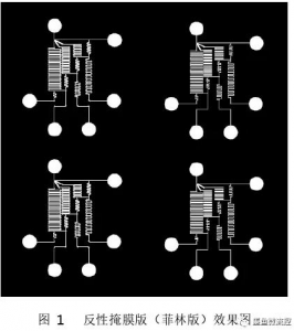
Before making die mold, we need to make a mask well in advance. The primary role is to block the specific area in the following photolithography process to transfer the design to a photoresist. The specific process is: first, using CAD software to design the layout of the chip structure drawing and save it as a DXF format file. The printer prints the microchannel pattern on the chip onto the plastic film. The plastic film material is photographic film. The transparent area on the negative mask is the microchannel section, and the opaque area is the non-channel portion, as shown in Figure 1.
Second, we need to pour the SU-8 photoresist onto the mold.
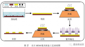
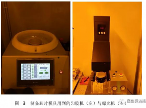
After the mask is made, the next step is to make the die mold to transfer the pattern on the mask to the silicon of SU-8 photoresist with a certain thickness. The process of graphics transfer generally includes the following steps: pretreatment, spin coating, pre-baking, exposure, after-baking, development, and hardening, the primary process as shown in Figure 2. In this paper, the male die is made in the ultra-clean room, in which the main equipment used is spin coater, developing machine, and programmable hot plate PHP-8, etc., equipment as shown in Figure 3.
(1) Pretreatment: NH4OHH2O2H2O (Ammonium hydroxide/hydrogen peroxide/deionized water) was mixed in a ratio of 1:1:5, the 4-inch silicon wafers were immersed in the mixture, and then the wafers were placed on a hot plate at 80 °C for 20 minutes. After soaking, the silicon wafer is rinsed repeatedly with deionized water and dried by a nitrogen gun. The purpose of this step is to remove the impurity particles on the surface of the silicon wafer and make the surface of the silicon wafer adhere better to the SU-8 photoresist.
(2) Spin coating: fix the pretreated silicon wafer on the tray in the spin coater to ensure the silicon wafer is located in the center of the tray. For the SU-8 photoresist in 100μm thickness, set the parameters of spin coater at 10s, 600RPM, then after 1min, set the parameter at the 40s, 1000RMP. Pour some SU-8 photoresist into the center of the silicon wafer and turn on the machine.
(3) Pre-baking: put the substrate on the hot plate at 65 °C for 5 minutes, then set at 95 ° °C for 10 minutes, then set hot plate temperature lower to 65 °C for 5 minutes again and finally to room temperature. The purpose of the step is to remove the solvent from the SU-8 photoresist by evaporation so that the photoresist on the silicon chip has better uniformity.
(4) UV exposure: place the cooled substrate under the exposure machine, and place the prepared negative mask on the substrate. The exposure dose for SU-8 photoresist of 100μm thickness is 3.6 MW/cm 2, and the exposure time is 35s.
(5) After-baking: place the exposed substrate on a hot plate at 65 ° C for 2 minutes, then set the hot plate to 95 ° C for 8 minutes, and finally to room temperature.
(6) Development: place the substrates respectively in an isopropyl alcohol solution for 15 seconds, until no white residue appears, and finally blow-dry with a nitrogen gun.
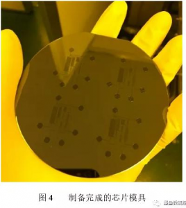
(7) Harden film: place the developed substrate in a vacuum drying box at 150 °C for 10 minutes to evaporate the remaining SU-8 photoresist solvent and make the SU-8 photoresist on the substrate adhere more firmly to the wafer. The fabrication of male die mold is finished, as shown in Figure 4.
For more information, you can connect us at elena@whchip.com or WhatsApp +8613884437686